
Technology
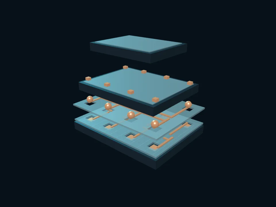
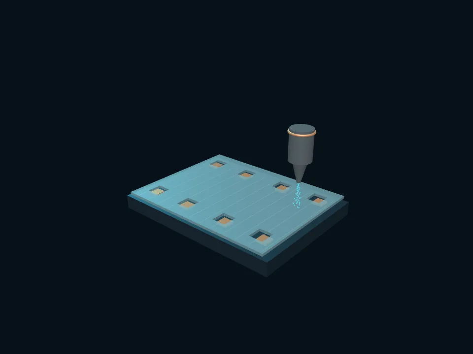
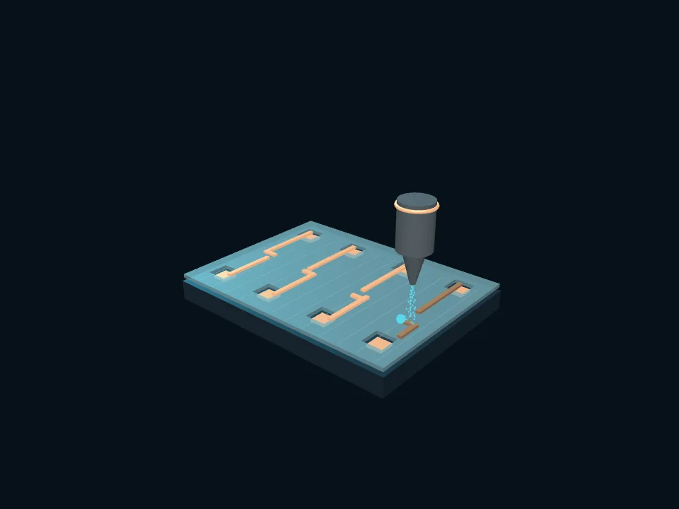
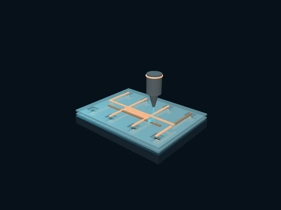
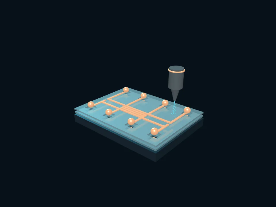
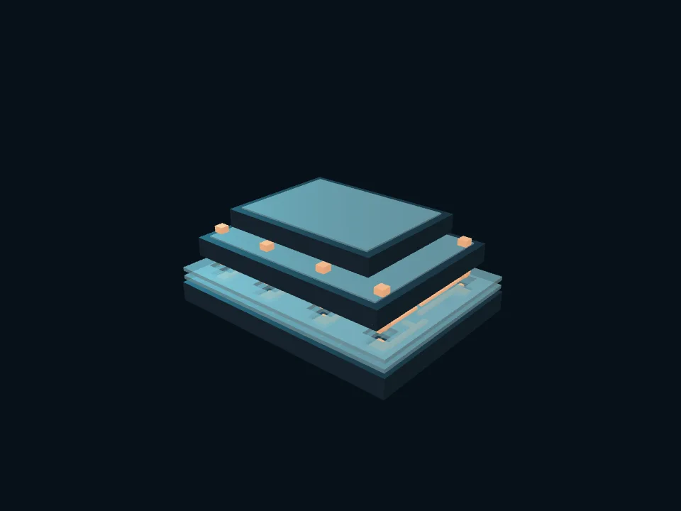
How the interposer is printed and how it differs from silicon interposers.
TechnologyApplications
Where small size meets small volumes: defence, medical technology, sensing.
ApplicationsExpert reports
What Fraunhofer ENAS, TU Dresden and Fraunhofer IFAM say about the process.
Expert reportsAdvantages over lithography
Free layout
Conductive structures and sensors in the micrometre range are printed directly onto the component.
Only tested chips in the stack
Each chip is tested and selected before stacking (known good die). This cuts scrap considerably.
Fast to market
A new layout needs no mask. The interposer is made in a single print run.
Changes by software
The layout comes straight from the CAD file. Changing the design only means changing the print job.
Less material
Material is applied only where it is needed. There is hardly any waste.
Lower equipment costs
Investment in lithography equipment is about three times as high as in equipment for aerosol jet printing.



Where we stand
The process is patented and has been assessed by three research institutes. There is no series production yet. We are looking for partners for pilot production and first applications.
+49 (0)89 74 88 810info@jp-microtech.de
To the contact form